The distribution of copper nucleation activities on a glassy carbon substrate
D. Torres1, M. Bernal1, J. Ustarroz1,2
1 ChemSIN – Chemistry of Surfaces, Interfaces and Nanomaterials, Université libre de Bruxelles
2 Research Group Electrochemical and Surface Engineering (SURF), Vrije Universiteit Brussel
jon.ustarroz@ulb.be
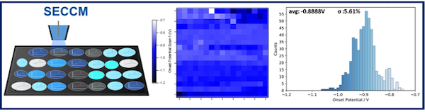
Electrochemical nucleation is a convenient strategy for the synthesis of functional nanostructures. As a heterogenous process, understanding the distribution of nucleation sites on a substrate is important since it relates the microscopic events to the macroscopic properties of the new deposit. Here, we have explored the electrochemical nucleation on a glassy carbon substrate with a local electrochemical approach based on the Scanning Electrochemical Cell Microscopy (SECCM), using copper as a case of study. The local approach allowed us to extract a statistically significant description of the nucleation process by performing hundreds of spatially-resolved experiments on different regions of the substrate. The diversity of nucleation sites can be characterized through a relevant magnitude such as the onset potential for nucleation. The spatially-resolved electrochemical characterization provides direct evidence of the diversity of nucleation sites on the substrate when monitored at the micro-scale, and opens up the opportunity to correlate the electrochemical information to the local surface state. Within this novel perspective, we further consider what renders a site active for nucleation by changing the local surface state with typical pretreatments of the substrate (i. e., polishing and preanodization) comparing the changes in the distribution of the onset potential for nucleation. The SECCM brings forward information on the electrochemical nucleation process that is simply unavailable with the conventional macro-scale approach. Nucleation sites distribution have a defining effect on the macroscopic properties of the deposit, therefore a comprehensive understanding and identification of such sites on a given substrate are essential to fabricate more advanced nanomaterials.